EWS100

Advanced Optical Inspection For Semiconductor Industry

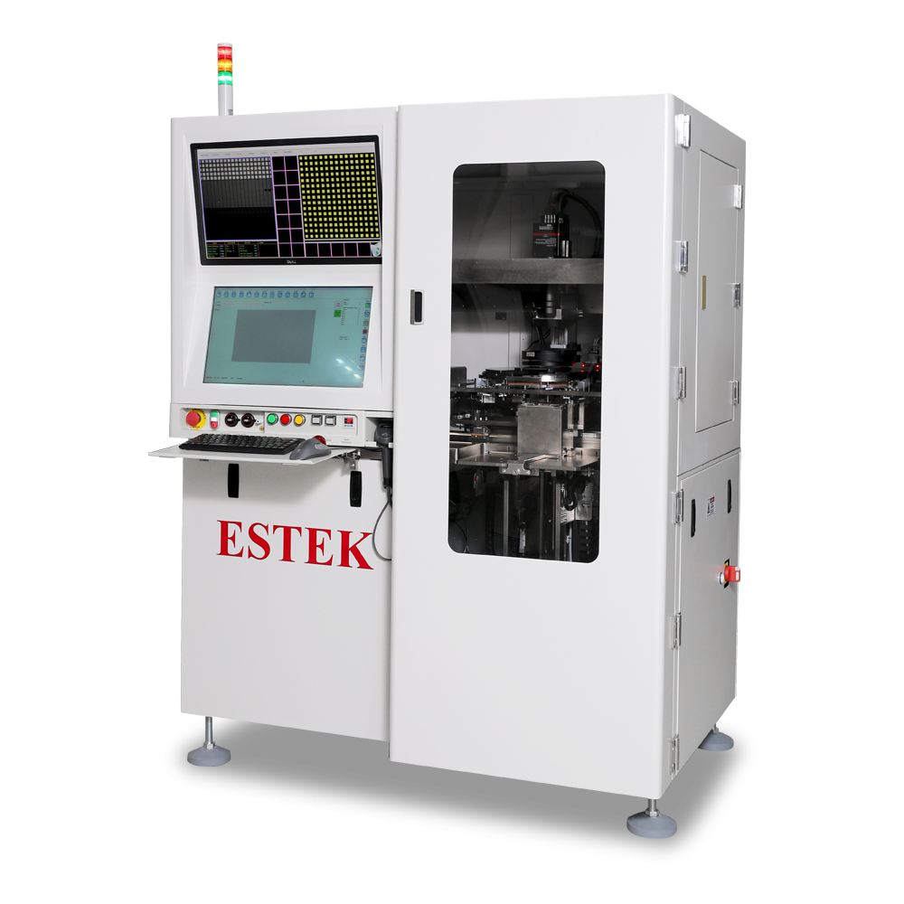
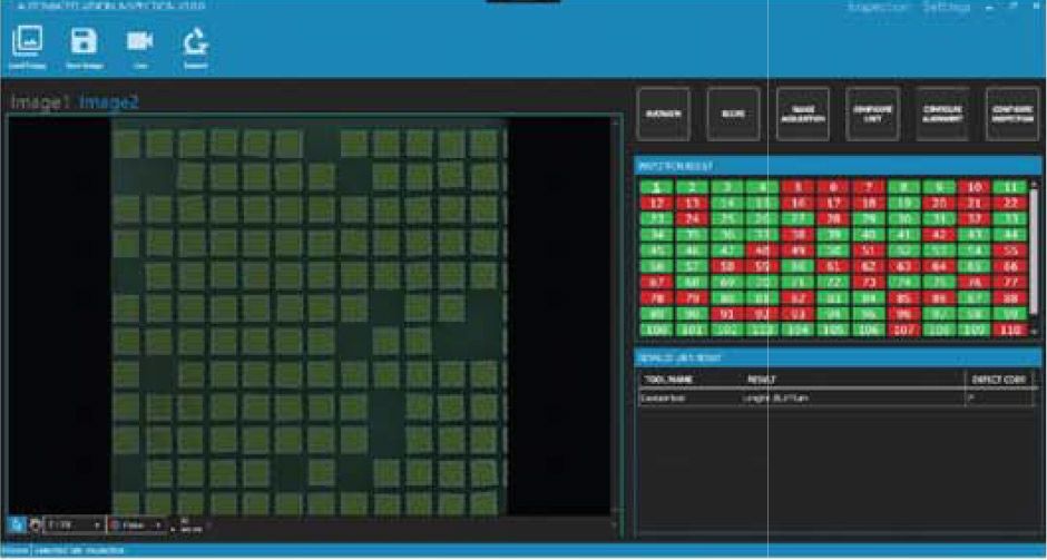
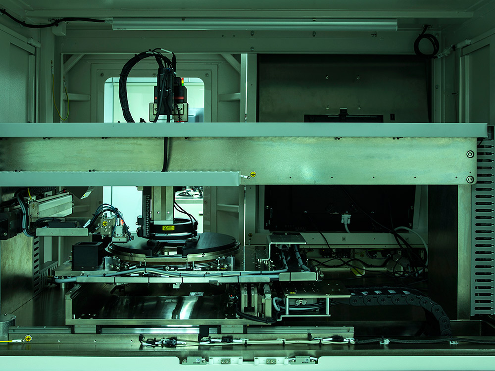
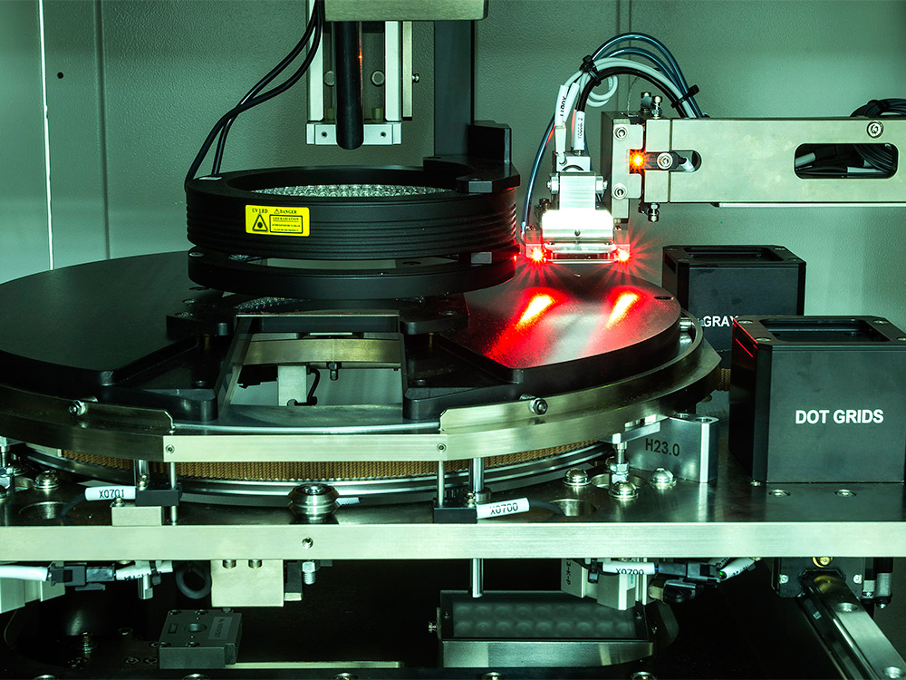
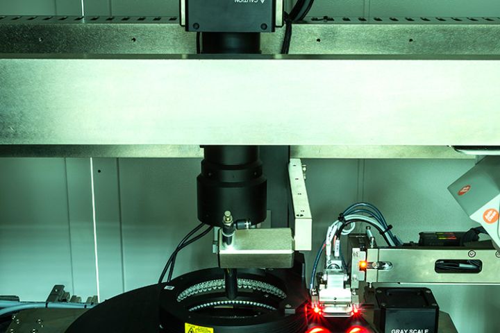
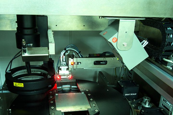
The EWS100 is a wafer inspection platform that leverages on ESTEK innovative Vision Technology. It delivers high-throughput and precision wafer-level and tile inspection.

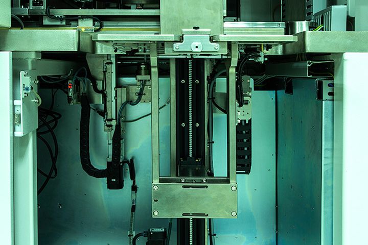
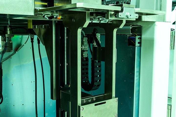
Advanced Motion couple with our vision systems provide dramatically improved positioning and alignment capability.User-friendly software improves efficiency and provides compatibility.

Estek provides dedicated inspection solutions to address the special requirements for LED manufacturing process

Specifications

Facilities

Voltage

220VAC Single Phase

Frequency

50/60 Hz

Power Comsumption

2.4KVA

Temperature
20 ~ 30°C
Humidity

18 ~70% RH Non-Condensing

CDA

6 Bar 200L/M

Camera

25M Color Camera
100M Color Camera with Pixel Shifting Technology
2um Resolution

Lens

Tele centric Lens

Lightings

Full Color RGB
Co-axial
Back Light

Wafer System

Wafer Size

4", 6", 8" and 12"

Wafer Handling

Gripper

Conversion time (Standard)

15 mins

Packages

Dimension (W x D x H)

1500 x 1200 x 2000mm 
(For 8" Wafer Only)

Weight (Net)

1300kg

Vision GUI - Mapping

For further information on our product & services

© 2019 by Estek Group. All Rights Reserved || CMS Web Design by AEIOU STUDIO