Specifications
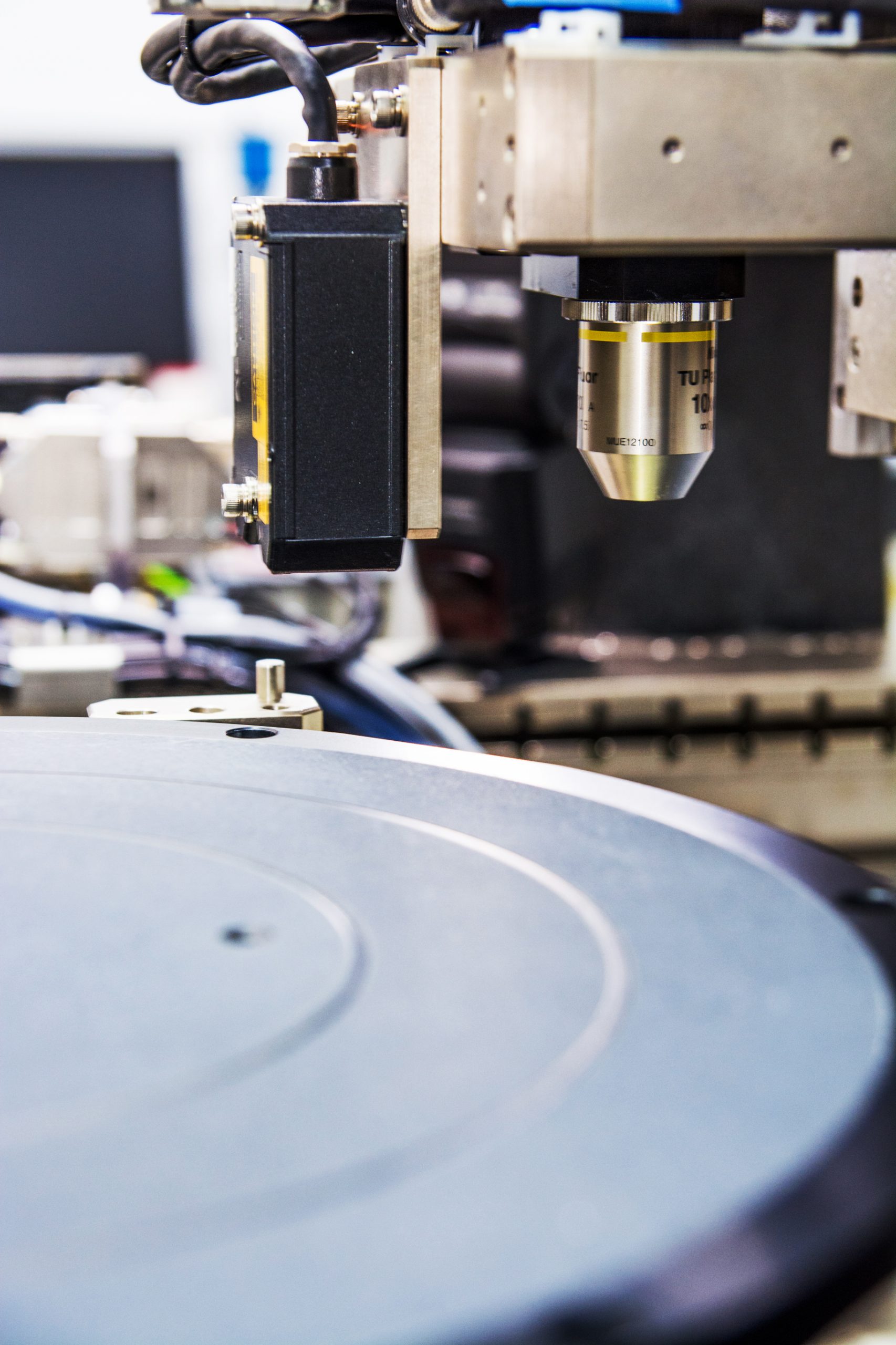
Inspection
Inspection Capabilities | Detecting wafer cosmetic defect, measurement, ink dot for wafer, probe mark & etc. |
Recipe / Setup (On and Off-Line) | Automatic “golden die” image generation from production wafer. |
Resolution | Changeable with multiple lens, up to 0.35µm per pixel. |
Accuracy | Up to 0.7µm. |
Repeatability | Up to 0.7µm at 3 sigma. |
Minimum Defect Detection | Up to 1µm. |